
To get the best experience for our site, we recommend you upgrade to the latest version of Internet Explorer, or select another web browser, a list of the most popular web browsers can be found below
You can download the main browser here:

Google Chrome

Firefox

IE11
 Position:
Home >
Products
> Fiber Optic Active Components
> Optical Transceivers
Position:
Home >
Products
> Fiber Optic Active Components
> Optical Transceivers
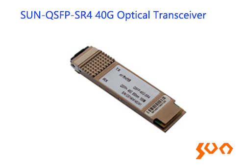
40G QSFP+Optical Transceiver, suitable for mutilmode OM3 Max distance 100m, OM4 Max 150m.

| PIN | Logic | Symbol | Name/Description | Notes |
| 1 | GND | Ground | 1 | |
| 2 | CML-I | Tx2- | Transmitter Inverted Data Input | |
| 3 | CML-I | Tx2+ | Transmitter Non-Inverted Data Input | |
| 4 | GND | Ground | 1 | |
| 5 | CML-I | Tx4- | Transmitter Inverted Data Input | |
| 6 | CML-I | Tx4+ | Transmitter Non-Inverted Data Input | |
| 7 | GND | Ground | 1 | |
| 8 | LVTLL-I | MODSEIL | Module Select | 2 |
| 9 | LVTLL-I | ResetL | Module Reset | 2 |
| 10 | VccRx | +3.3V Power Supply Receiver | ||
| 11 | LVCMOS-I/O | SCL | 2-Wire Serial Interface Clock | 2 |
| 12 | LVCMOS-I/O | SDA | 2-Wire Serial Interface Data | 2 |
| 13 | GND | Ground | 1 | |
| 14 | CML-O | Rx3+ | Receiver Non-Inverted Data Ouput | |
| 15 | CML-O | Rx3- | Receiver Inverted Data Ouput | |
| 16 | GND | Ground | 1 | |
| 17 | CML-O | Rx1+ | Receiver Non-Inverted Data Ouput | |
| 18 | CML-O | Rx1- | Receiver Inverted Data Ouput | |
| 19 | GND | Ground | 1 | |
| 20 | GND | Ground | 1 | |
| 21 | CML-O | Rx2- | Receiver Inverted Data Ouput | |
| 22 | CML-O | Rx2+ | Receiver Non-Inverted Data Ouput | |
| 23 | GND | Ground | 1 | |
| 24 | CML-O | Rx4- | Receiver Inverted Data Ouput | 1 |
| 25 | CML-O | Rx4+ | Receiver Non-Inverted Data Ouput | |
| 26 | GND | Ground | 1 | |
| 27 | LVTTL-O | ModPrsL | Module Present | |
| 28 | LVTTL-O | IntL | Interrupt | 2 |
| 29 | VccTx | +3.3 V Power Supply Transmitter | ||
| 30 | Vcc1 | +3.3 V Power Supply | ||
| 31 | LVTTL-I | LPMode | Low Power Mode | 2 |
| 32 | GND | Ground | 1 | |
| 33 | CML-I | Tx3+ | Transmitter Non-Inverted Data Input | |
| 34 | CML-I | Tx3- | Transmitter Inverted Data Input | |
| 35 | GND | Ground | 1 | |
| 36 | CML-I | Tx1+ | Transmitter Non-Inverted Data Input | |
| 37 | CML-I | Tx1- | Transmitter Inverted Data Input | |
| 38 | GND | Ground | 1 |
| Parameter | Symbol | Min | Max | Units |
| Storage Temperature | Tst | -20 | 85 | degC |
| Input Voltage | Vin | -0.3 | Vcc+0.3 | V |
| Operating Case Temperature | Top | 0 | 70 | degC |
| Power Supply Voltage | Vcc | -0.3 | 3.6 | V |
| Relative Humidity (non-conensation) | RH | 5 | 95 | % |
| Parameter | Symbol | Min | Typical | Max | Units |
| Operating Case Temperature | Tca | 0 | 70 | degC | |
| Power Supply Voltage | Vcc | 3.13 | 3.3 | 3.47 | V |
| Date Rate, Each Lane | 10.3 | 10.5(1) | Gb/s | ||
| Power Dissipation | Pm | 1.5 | W | ||
| Fiber Bend Radius | Rb | 3 | CM | ||
| Link Distance (OM3 MMF) | D1 | 100 | M | ||
| Link Distance (OM4 MMF) | D2 | 150 | M |
| Parameter | Symbol | Min | Typical | Max | Units | Notes |
| Power Consumption | 3.5 | W | ||||
| Differential Input Impedance | Zin | 90 | 100 | 110 | Ohm | |
| Differential Output Impedance | 90 | 100 | 110 | Ohm | ||
| Differential input voltage Amplitude | ΔVin | 300 | 1100 | mVpp | ||
| Differential output voltage Amplitude | Out | 500 | 800 | mVpp | ||
| Skew | Sw | 300 | ps | |||
| Bit Error Rate | BER | E-12 | ||||
| Input Logic Level High | VIH | 2 | VCC | V | ||
| Input Logic Level Low | VIL | 0 | 0.8 | V | ||
| Output Logic Level High | VOH | VCC-0.5 | VCC | V | ||
| Output Logic Level Low | VOL | 0 | 0.4 | V |
| Parameter | Symbol | Min | Typical | Max | Units | Notes |
| Transmitter | ||||||
| Center Wavelength | λC | 840 | 850 | 860 | nm | |
| RMS Spectral Width | ∆λ rms | 0.65 | nm | |||
| Average Launch Power, Each Lane | Pavg | -7.5 | 2.5 | dBm | ||
| Difference in Launch Power between any Two Lanes (OMA) |
4 | dBm | ||||
| Extinction Ratio | ER | 3 | dB | |||
| Peak power, Each Lane | 4 | dBm | ||||
| Transmitter and Dispersion Penalty (TDP), Each Lane |
TDP | 3.5 | dB | |||
| Transmitter Eye Mask Definition {X1, X2, X3, Y1, Y2, Y3} | {0.23, 0.34, 0.43, 0.27, 0.35, 0.4} | Hit Ratio = 5x10⁻⁵ | ||||
| Average Launch Power OFF Transmitter, Each Lane | -30 | dB | ||||
| Receiver | ||||||
| Center Wavelength | λC | 840 | 850 | 860 | Nm | |
| Minimum Average Receive Power, Each Lane | -9.5 | dBm | ||||
| Receiver Reflectance | Rr | -12 | dB | |||
| Maximum Average Receive Power, Each Lane | 2.4 | dBm | ||||
| Stressed Receiver Sensitivity (OMA), Each Lane | -5.4 | dBm | 1 | |||
| Peak Power, Each Lane | 4 | dBm | ||||
| LOS Assert | LOSA | -30 | dBm | |||
| LOS De-Assert-OMA | LOSD | -7.5 | dBm | |||
| LOS Hysteresis | LOSH | 0.5 | dB | |||
| Model | Name | Description |
| SUN-QSFP-40G-SR4 | SFP Module | QSFP+ SR4, 100m on OM3 Multimode Fiber (MMF)and 150m on OM4 MMF;0 to +70°C |
| SUN-QSFP-40G-SR4-I | SFP Module | QSFP+ SR4, 100m on OM3 Multimode Fiber (MMF)and 150m on OM4 MMF;-40 to +85°C |
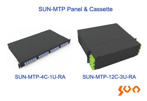
SUN-MTP Panel & Cassette
Model: SUN-MTP
19 " Standard rack structure, rack height 1U/4U, big capacity
Features
 Easy to install and operate 19-inch standard structure High density, large capacity
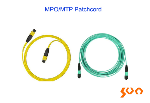
SUN-MPO Fiber Optic Patchcord
Model: SUN-MPO
Features
Low insertion loss High return loss Good durability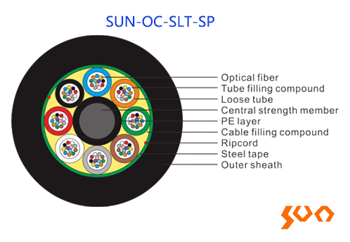
SUN-OC-SLT-SP Stranded Loose Tube Light-armored (Steel Tape) Cable (GYTS)
Model: SUN-OC-SLT-SP
GYTS, Loose Tube Light-armored (Steel Tape) Cable, 2-144cores
Features
Good mechanical and temperature performance High hydrolysis resistance and high strength loose tube Good crush resistance and flexibility High tensile strength ensured by steel wire Good moisture-proof ensured by PSP Gopher protected cable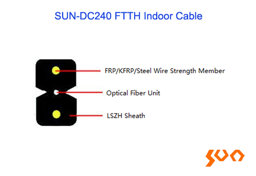
SUN-DC240 FTTH Indoor Cable
Model: SUN-DC240
Drop Cable, 1-4 cores, G657, flame retardent, for FTTH application
Features
Good crush resistance ensured by parallel strength member Good tensile strength ensured by single steel wire Low smoke, zero halogen and flame retardant sheath Simple Structure, light weight and high practicability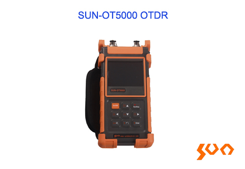
SUN-OT5000 OTDR
Model: SUN-OT5000
Can test SM and MM fibers, optional light source, VFL and power meter
Features
Quick startup FTTX in-service testing (Up to1:64 splitter) Built-in PON power meter for Triple-play testing High configuration series include optical light source, optical power meter, visual fault locator (VFL) and Optical Connector Inspector (MCI) modules USB data interface (PC software for batch data processing and report output) Dustproof and shockproof (2-meter drop test) Light weight, small size, rugged design and simple operation Visual link image software (Optional)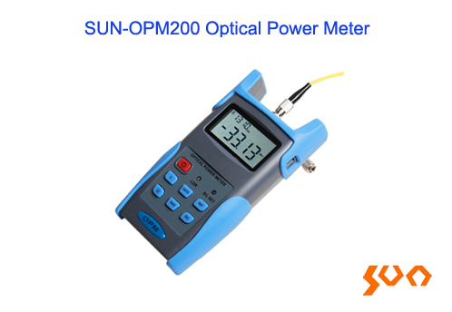
SUN-OPM200 Optical Power Meter
Model: SUN-OPM200
FC ⁄ SC ⁄ ST, REF, backlight control, USB port
Features
User self-calibration function Power measurements in dBm or mW Auto power off after 10 minutes without operation Standard FC/SC/ST interchangeable port Backlight LCD display for night operation REF setting function Intelligent backlight control Auto wavelength and frequency identification High storage capacity USB communication port for data transfer


 ics@suntelecom.cn
  +86 18964888554
 Building No.145, Lane 666 Xianing Road, Jinshan Industrial Zone, Shanghai 201506, China
Copyright ©1989-2025 ALL Rights Reserved
ICP (Shanghai) Number: 13005159


 +86 21 60138638
 suntelecom.s02